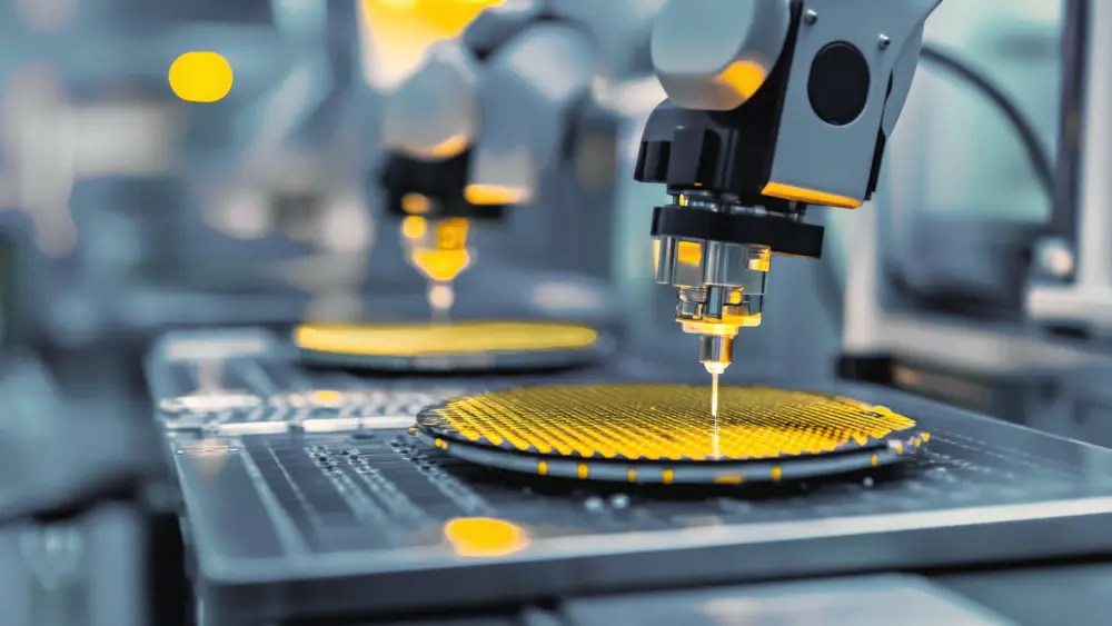
半导体和电子产品的表面测量技术
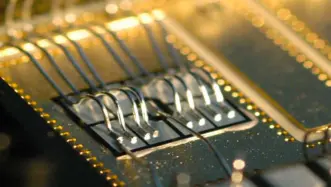
随着半导体器件日益微型化以及封装技术日益复杂,半导体制造商需要在整个生产过程中采用非接触式、纳米级精度的表面测量技术。TopMap 白光干涉测量(WLI)技术可对表面进行快速、高精度的三维测量,且不会造成碰撞或损坏表面结构。
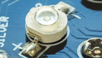
TopMap 轮廓仪为晶圆、MEMS、先进封装及电子产品提供测量解决方案,通过纳米级分辨率的表面形貌、台阶高度、粗糙度、平整度、翘曲及厚度测量,实现可靠的质量控制、工艺优化和失效分析。
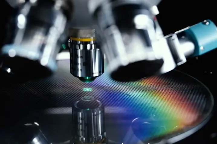
TopMap 3D 轮廓仪在半导体领域的应用
- 测量硅片尺寸、硅片平整度,表征弯曲和翘曲特征,或表面波纹度(包括化学机械抛光(CMP)后的表面粗糙度)。
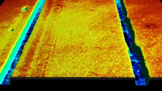
- 对化学机械抛光(CMP)后的硅片进行检测,检查残留台阶高度、划痕和缺陷,以及抛光后的表面粗糙度。
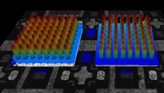
- 检查微凸点和焊料凸点,重点关注凸点高度、引脚共面度及圆度。
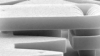
- MEMS和微电子器件的变形、微镜平整度、表面粗糙度及蚀刻深度
- 检测TSV的深度和VIA的直径,包括对凹陷区域或VIA周围表面平整度的测量。

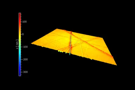
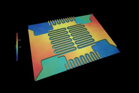
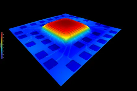


用于电子和半导体行业的光学轮廓仪和振动计
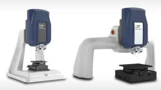
三维光学轮廓仪
Micro.View 系列三维光学轮廓仪专为亚纳米级分辨率测量而优化。凭借聚焦光学系统与高垂直分辨率,可对微观结构、表面光洁度及材料分布进行精细分析——在最微小的偏差都可能影响性能的场景中,提供可靠的数据支撑。
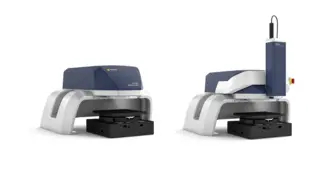
大视场三维光学轮廓仪
Pro.Surf 可对大型工件及多样本料盘进行平面度、台阶高度与平行度检测——非接触、数秒完成。防碰撞远心光学系统可深入深孔内部进行测量,满足生产环节对精度与重复性的严苛要求。
显微式激光测振仪
随着微机电系统和MEMS快速发展,Polytec推出了高度创新的显微式测量系统产品线。Polytec的MSA系列显微式激光测振仪带宽可达数kHz,数MHz,甚至数GHz,以最高精度可靠地验证微系统的动力学特性和轮廓数据。MSA集多功能于一体,可用于确定传递函数、表征微器件的3D静态和动态特性,甚至可透过封装好的硅帽,获取其在工作条件下的整个层制结构。
放心选择适合您的表面轮廓仪,尽享“先试后买”服务






为何在半导体和电子领域使用白光干涉测量技术
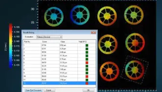
白光干涉测量技术将卓越的垂直分辨率与快速、非接触式测量相结合。Sherpa 软件中的引导式工作流程有助于实现流程自动化并加快操作速度,而高重复性和可靠的测量结果则能够满足周期时间要求及更高吞吐量的需求。与接触式轮廓仪或传统光学显微镜相比,TopMap 白光干涉仪能在更短时间内提供更深入的洞察。

为什么白光干涉仪是半导体计量领域的首选解决方案
WLI的亚纳米级垂直分辨率揭示了真实的3D表面形貌
可测量从哑光、深色到光亮、抛光及镜面般光滑的晶圆,包括反射率变化的晶圆
用于过程控制的高速、高重复性测量,并配备面向生产的自动分析功能